Introduction
Electromagnetic interference (EMI) shielding is a critical part of achieving EMC compliance. However, in real-world product design, failures are rarely caused by poor material selection alone.
In many cases, improper grounding, structural gaps, and cable coupling effects are the real reasons why shielding fails—or even makes emissions worse.
This guide outlines the most common EMI shielding problems, their root causes, and practical engineering solutions based on real-world scenarios.
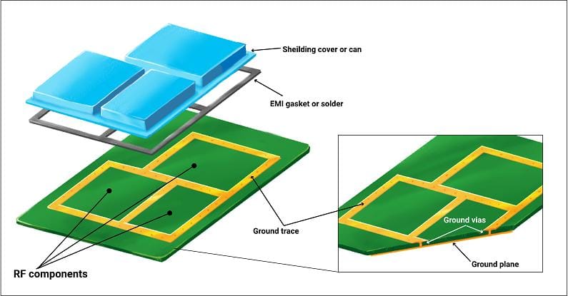
1. Poor Grounding: When Shielding Becomes an Antenna
Symptoms
- Radiated emissions increase after adding a metal enclosure
- EMI test results worsen by 10–20 dB or more
Root Cause
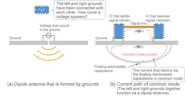
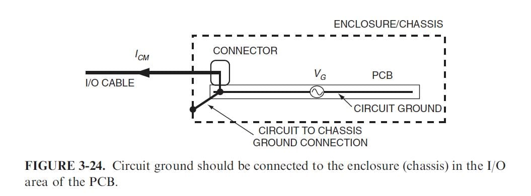
If the shielding enclosure is not properly connected to the system ground (0V reference), it becomes a floating conductor.
This creates parasitic capacitance between:
- Internal circuits → enclosure
- Enclosure → external cables
As a result, noise is coupled onto cables, turning them into efficient antennas.
Solution
- Ensure low-impedance grounding between PCB ground and enclosure
- Use multiple grounding points (not a single screw)
- Minimize ground loop inductance
✔ Design Rule
- Keep grounding impedance as low as possible (<10 mΩ recommended)
- Use via stitching around shield boundaries
2. Gaps and Seams: The Hidden Leakage Path
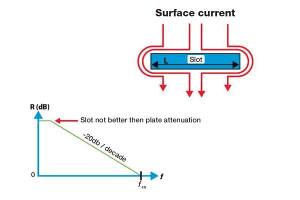
Symptoms
- Shielding effectiveness is much lower than expected
- High-frequency leakage from enclosure edges
Root Cause
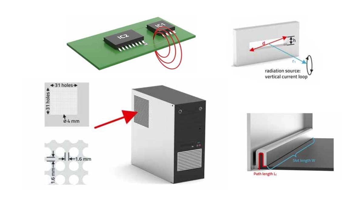
Any gap or seam acts like a slot antenna.
When the gap size approaches λ/20 of the interference wavelength, significant radiation leakage occurs.
Solution
- Minimize seam width and length
- Use conductive gaskets or EMI foam
- Add dense grounding vias along seams
✔ Design Rule
- Gap size < λ/20 of the highest frequency
- Increase contact points to reduce contact resistance
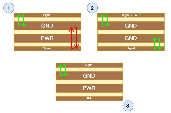
3. Poor PCB Layout and Stack-Up Design
Symptoms
- EMI persists even after shielding
- Unexpected coupling or noise issues
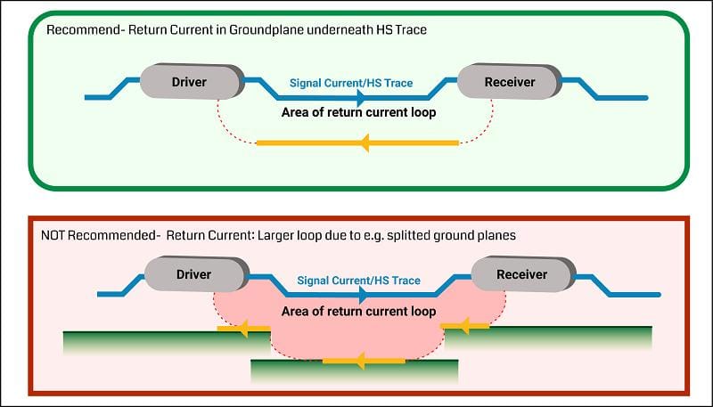
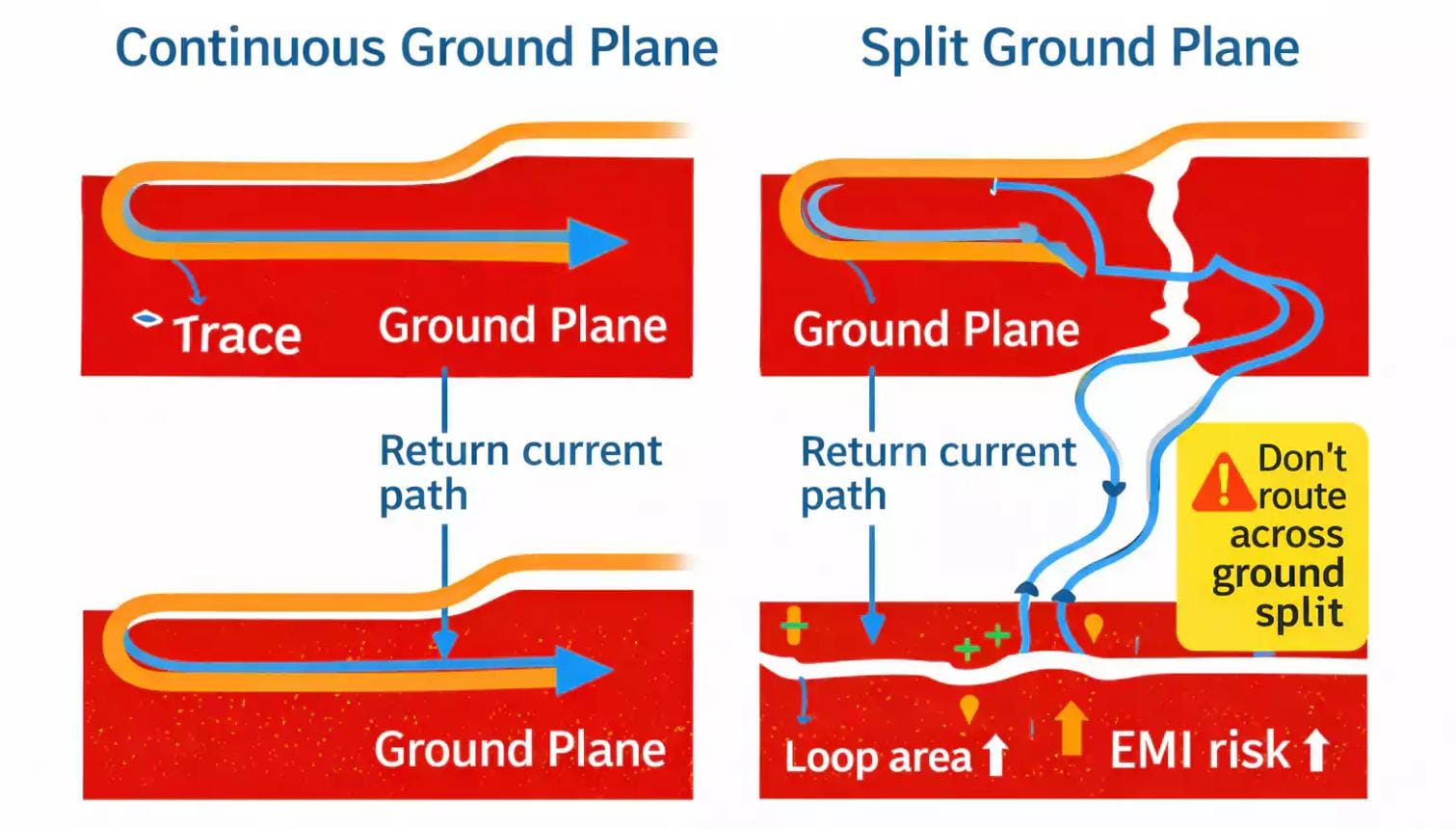
Root Cause
❌ Discontinuous Return Paths
High-frequency current always follows the lowest inductance path (directly under the signal trace).
If the reference plane is split, current detours and creates large loop areas → radiation sources.
❌ Poor Stack-Up
Signal layers not adjacent to ground planes increase field spread and coupling.
❌ Mixed Layout Zones
Digital, power, and RF circuits share the same area → noise coupling.
Solution
- Use proper stack-up:
Signal – Ground – Signal – Power – Ground – Signal - Ensure continuous ground planes under high-speed signals
- Separate noisy and sensitive circuits
✔ Design Rule
- Never route high-speed signals across split planes
- Add stitching vias when changing layers
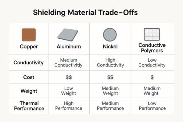
4. Wrong Shielding Material Selection
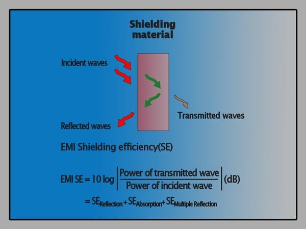
Symptoms
- Shielding ineffective at certain frequencies
- Performance degrades over time
Root Cause
❌ Frequency Mismatch
- High-frequency EMI → needs conductive materials (Cu, Al)
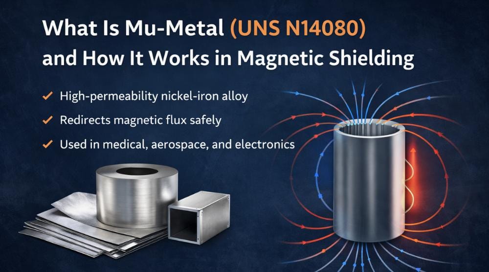
- Low-frequency magnetic fields (<1 MHz) → require high-permeability materials
❌ Insufficient Thickness
If thickness < skin depth, EMI penetrates the shield.
❌ Poor Conductive Coating
- Uneven thickness
- Oxidation
- Poor adhesion
Solution
- Select material based on frequency range
- Ensure proper thickness and plating quality
- Perform adhesion and reliability testing
✔ Design Rule
- High frequency → Copper / Aluminum
- Low frequency → Mu-metal / Ferrite
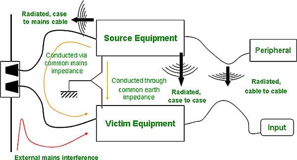
5. Cable Coupling: The Most Overlooked EMI Source
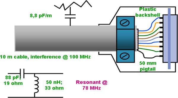
Symptoms
- System passes test without enclosure but fails with enclosure
- Long cables radiate strong EMI
Root Cause
Cables act as unintentional antennas.
Noise coupling path:
- Internal circuit → enclosure (parasitic capacitance)
- Enclosure → cable
- Cable radiates EMI
Solution
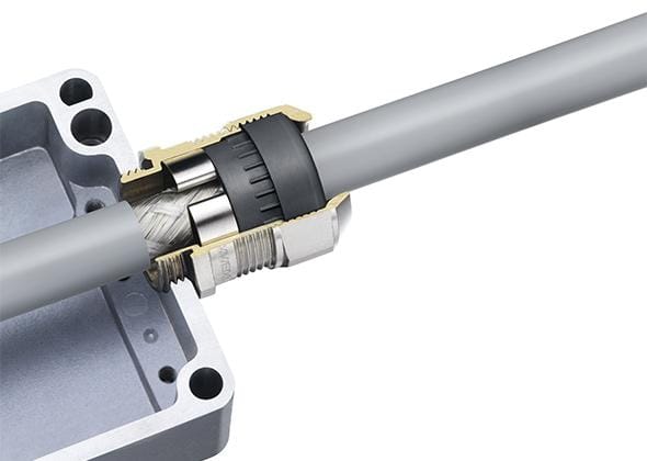
- Ground shield at cable entry points
- Use shielded cables
- Add ferrite cores if needed
✔ Design Rule
- Keep cable length as short as possible
- Ensure proper cable shield termination
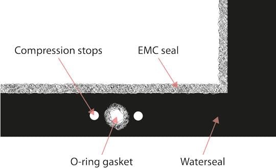
6. Assembly and Manufacturing Issues
Symptoms
- Prototype passes, mass production fails
- Performance degrades over time
Root Cause
- Misaligned conductive gaskets
- Over-compression → material damage
- Poor soldering of shielding cans
Solution
- Use positioning fixtures for assembly
- Design compression limits into structure
- Perform quality inspection (e.g., X-ray for solder joints)
✔ Design Rule
- Control compression ratio of conductive materials
- Standardize assembly process
Real Case Study: When Shielding Makes EMI Worse
A power supply product was fully enclosed in a metal housing.
However, during EMC testing (based on CISPR standards), radiated emissions exceeded limits.
Surprisingly, removing the enclosure made the product pass.
Root Cause
- The enclosure was not grounded
- It became a floating conductor
- Noise coupled to cables → cables radiated EMI
Lesson Learned
EMI shielding is not just about adding metal—it’s about controlling current paths.
Key EMI Shielding Design Checklist
✔ Ensure low-impedance grounding between PCB and enclosure
✔ Keep seams and gaps < λ/20
✔ Maintain continuous return paths
✔ Separate noisy and sensitive circuits
✔ Select materials based on frequency
✔ Control cable radiation paths
✔ Validate assembly consistency
How We Can Help
If you’re facing EMI/EMC failures, the issue is often not just materials—but system-level design flaws.
We provide:
- EMI shielding materials (copper foil tape, aluminum foil tape, conductive adhesives)
- Engineering support for shielding design optimization
- Custom solutions for complex EMC challenges
Feel free to contact our team for technical support or material recommendations.