Product Description
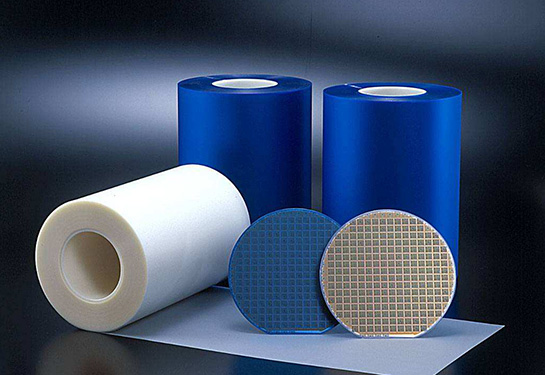
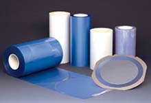
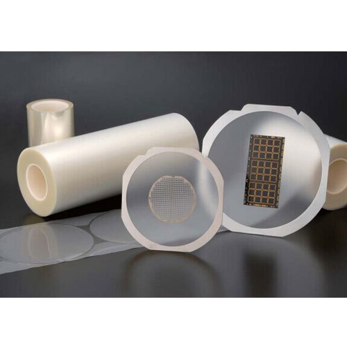
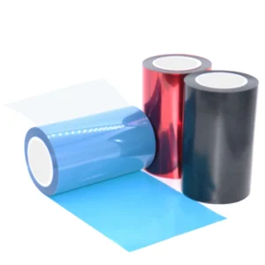
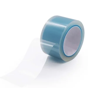
UV release protective film is a high-performance PET-based tape coated with special UV-curable acrylic adhesive. Before exposure, it provides strong adhesion for secure fixing; after UV irradiation, adhesion drops dramatically, allowing easy removal without residue. This film is widely used in semiconductor wafer processing, FPCB manufacturing, LCD/OLED panel protection, and other precision electronic applications where accurate positioning and efficient processing are required.
Specifications
| Product Code Technical Parameters | KA4640 | KA4611 | KA4662 | KA4616 | KA4618 |
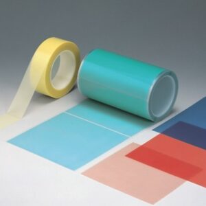
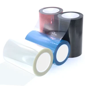
| Color | Translucence | Translucence | Translucence | Translucence | Translucence |
| Total Thickness[mm] | 0.08 | 0.11 | 0.155 | 0.16 | 0.16 |
| Backing Thickness[mm] | 0.05 | 0.1 | 0.14 | 0.14 | 0.14 |
| Backing | PET | PET | PO | PO | PO |
| Adhesive | Acrylic | Acrylic | Acrylic | Acrylic | Acrylic |
| 180°Peel Strength (Before UV )[N/inch] | 20 | 8 | 12 | 10 | 20 |
| 180°Peel Strength (After UV )[N/inch] | 0.05~0.1 | 0.03~0.06 | 0.15~0.25 | 0.3~0.5 | 0.05~0.1 |
| UV Exposure Rate[mJ/cm2] | 300~500mJ | 300~500mJ | 300~500mJ | 300~500mJ | 300~500mJ |
| Application | Glass | Glass | MEMS CHIPS | Ceramics | wafer |
Features
Rapid adhesion reduction after UV exposure for efficient release
Stable adhesion and accurate positioning without surface damage
High transparency for optical inspection and automated production
Anti-static treatment to minimize dust contamination
Excellent heat and chemical resistance for precision processes
Applications
Semiconductor wafer dicing and chip processing
FPCB (Flexible Printed Circuit Board) handling and processing
LCD and OLED glass panel protection
Optical components and touchscreen manufacturing
Precision electronic parts transport and surface protection
Reviews
There are no reviews yet.